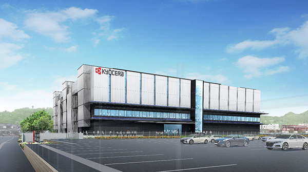
Kyocera Corporation (President: Hideo Tanimoto, hereafter “Kyocera”) today announced it will begin construction of a new research and development center in January 2021 at its Kokubu campus in Kirishima City, Kagoshima, Japan. Kyocera has executed a location agreement with the mayor of Kirishima City for the new R&D center, which will focus on new innovations in the fields of information and communications, environmental preservation, and smart energy.

Architect’s rendering of a new R&D center
The Kokubu campus is already an innovation hub and site of three strategic R&D groups: Kyocera’s Monozukuri R&D Laboratory, which focuses on advanced material technologies; its Production Technology Division, focusing on manufacturing process innovation; and its Analysis Center, which develops simulation and evaluation technologies. R&D programs at the campus currently include 5G smartphone technologies, electronic and semiconductor components used in IoT devices, and key components for new smart energy technologies, such as cell stacks for Solid Oxide Fuel Cells (SOFCs). Intellectual property developed there has found a wide range of other applications as well, in the automotive, aerospace, medical and healthcare fields.
Through greater collaboration among these R&D operations, Kyocera will establish a new platform to accelerate development and production efforts, with comprehensive support for manufacturing new products, promoting factory automation, and improving manufacturing efficiencies. Kyocera will position the new facility specifically as an incubator for open innovation, sharing technical information for human resource development, and networking with inventors outside of Kyocera.
| Name | (To be announced) |
| Location | Kyocera’s Kagoshima Kokubu Plant Campus 1450-1 Azadainomaru, Kokubukamikogawa, Kirishima-shi, Kagoshima Prefecture, Japan |
| Total investment | Approximately 10 billion yen (approx. 96 million U.S. dollars) |
| Building area | 5,990 m2 steel construction with 5 stories |
| Total floor space | 22,902 m2 |
| Construction plan | Construction begins: January 2021 Facility opens: September 2022 |
| Main R&D activities | Development of laminated ceramic capacitors, ceramic packages for electronic devices, cell stacks for SOFCs |
Sources from: https://global.kyocera.com/news/2020/1204_icjm.html
Declaration: This article is provided by CERADIR™ users or obtained from Internet, the content does not represent the position of CERADIR™. We are not responsible for the authenticity/accuracy of the article, especially the effects of the products concerned. This article is for study only, it does not constitute any investment or application advice. For reprinting, please contact the original author. If it involves the copyright and/or other issues, please contact us and we will deal with it asap! CERADIR™ has the interpretation of this declaration.


